


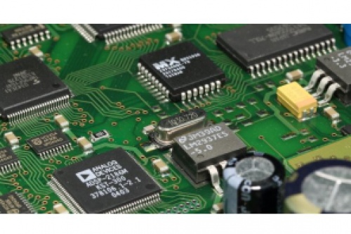
PCBs are critical components of electronic devices, used in a wide range of applications from consumer electronics to aerospace and defense. As such, ensuring the quality and reliability of PCBs is essential to their successful operation. PCB testing and inspection are key steps in this process, and PCB design services can provide valuable expertise in these areas.
PCB Testing
PCB testing is the process of verifying that a PCB meets its design specifications and operates correctly. There are several types of PCB testing, including:
Visual inspection: This involves examining the PCB for defects such as missing or misaligned components, solder bridges, and other assembly issues. Visual inspection can be done manually or with the help of automated systems.
Electrical testing: This involves applying power and signals to the PCB and measuring the resulting responses. Electrical testing can detect issues such as open circuits, short circuits, and incorrect component values.
Functional testing: This involves testing the PCB in its intended application or environment. Functional testing can verify that the PCB performs as expected and meets its design requirements.
PCB Inspection
PCB inspection is the process of examining a PCB to identify defects or other issues that may impact its performance or reliability. There are several types of PCB inspection, including:
X-ray inspection: This involves using X-rays to examine the internal structure of a PCB. X-ray inspection can detect issues such as hidden solder joints, voids, and other defects that are not visible with visual inspection.
Automated optical inspection (AOI): This involves using cameras and software to automatically inspect PCBs for defects such as missing or misaligned components, solder bridges, and other assembly issues.
In-circuit testing (ICT): This involves using test probes to measure the electrical characteristics of a PCB while it is in operation. ICT can detect issues such as open circuits, short circuits, and incorrect component values.
PCB Layout Services
One key area where PCB layout services can provide value is in the design of test points and test pads. These are points on the PCB where test probes can be attached for electrical testing. Proper placement and design of test points and test pads can facilitate testing and ensure that all critical electrical characteristics are measured.
Another area where PCB layout services can provide value is in the design of PCBs for manufacturability. Designing a PCB with manufacturability in mind can help reduce the risk of defects and improve the efficiency of the assembly process. This can result in lower costs and improved reliability.
CAD Drawing
CAD drawing services can also be useful in PCB testing and inspection. CAD (computer-aided design) is used to create the schematics and layouts for PCBs, and CAD drawings can be used for visual inspection and verification of the PCB design. CAD drawing services can also be used to create 3D models of the PCB and its components, which can be used for simulation and testing.
PCB testing and inspection are critical steps in ensuring the quality and reliability of PCBs. PCB design services, PCB layout services, and CAD drafting services can provide valuable expertise in these areas, helping to ensure that a PCB meets its design specifications and operates correctly in its intended application or environment.